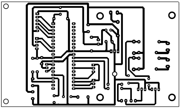
Many times, a PCB layout (as discussed in chapter VII, Let’s Talk about Circuit Boards) and a schematic diagram are often interchanged in circuitry; it has led others, especially the novices in circuit engineering, to believe that they are one and the same. In a way, since they are both presentations of a circuit’s system, they may seem similar. However, upon closer inspection, they are not. It is, therefore, essential in the circuit design process that the difference is acknowledged.
A PCB layout is a physical representation or a real model of a circuit. It presents all of the electrical components that are included; it also details which of the components are active and which ones are passive. Although it can show an actual working circuit, understanding the functions of each of its parts can be tedious.

A PCB layout is an actual circuit model
On the other hand, a schematic diagram, also called simply as a circuit diagram, is a descriptive outline of a circuit’s system; it is the standard and less costly way of circuit representation. It is like a PCB layout that shows both of the active and passive components in a circuit; unlike a PCB layout, however, its presentations can be easily understood.

A schematic diagram can include important notes for the improvement of a circuit’s design
Stages of circuit design:
Meeting specific requirements The creation of a circuit diagram
Building a breadboard, or a PCB layout
The presentation of each circuit component (for professional evaluation) Applying the results of evaluation
Testing (and retesting)
Getting approval from professionals
Circuit design tips for beginners (preparation process): Categorize the components
Construct a PCB layout, as well as a schematic diagram Determine the compatibility of each circuit component
Circuit design tips for beginners (circuit-building process): Always avoid cold solder joints
Always separate power controls and other connections Always separate analog and digital components
Create traces should hard-to-find components be included Remember to always make integral nodes accessible
Solder the components systematically; solder small components first, then, solder larger components next
Strategize the spaces you allow between components Take note of any heat spots
Related Articles
Lesson meta keywords and meta description:
Write a public review