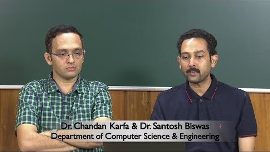
Optimization Techniques for Digital VLSI Design free videos and free material uploaded by Guwahati Staff .
Module 1: Introduction and High-level Synthesis
Lecture 1: Introduction to Digital VLSI Design Flow
Lecture 2: High-level Synthesis (HLS)
Lecture 3: Impact of Compiler Optimizations on HLSLecture 4: Heuristic based Optimization Techniques for HLS
Module 2: Logic Synthesis and Physical Synthesis
Lecture 1: Introduction to Logic Synthesis and Physical Synthesis
Lecture 2: 2-level Logic optimization, multi-level Logic optimizations
Lecture 3: Heuristic based logic optimization: EXPRESSO
Lecture 4: Optimization Techniques for Physical SynthesisLecture 5: DSP and RAM inference for FPGA
Module 3: RTL Optimizations
Lecture 1: Retiming for Clock period minimization
Lecture 2: Register balancing, FoldingLecture 3: Pipelining, Replication, Clock Gating
Module 4: VLSI Testing
Lecture 1: Introduction to Digital VLSI Testing, Automatic Test Pattern Generation (ATPG), Design for Testability
Lecture 2 and 3: Optimization Techniques for ATPG
Lecture 4: Optimization Techniques for Design for Testability
Lecture 5: High-level fault modelingLecture 6: RTL level Testing
Module 5: Verification
Lecture 1: LTL/CTL based Verification
Lecture 2: Verification of Large Scale Systems
Lecture 3: BDD based verification
Lecture 4: ADD based verification, HDD based verification
Lecture 5: Symbolic Model CheckingLecture 6: Bounded Model Checking
Digital VLSI Design flow comprises three basic phases: Design, Verification and Test. This course will give a brief overview of the VLSI design flow. The primary emphasis of the course is to introduce the important optimization techniques applied in the Industry level electronic design automation (EDA) tools in the VLSI design flow. This course is unique in the sense that it will give a comprehensive idea about the widely used optimization techniques and their impact the generated hardware.
The outline of the course is as follows:
VLSI Design: Overview of digital VLSI design flow; High-level Synthesis, logic synthesis and physical synthesis and optimization techniques applied in these three steps; Impact of compiler optimization on hardware synthesis, 2-level logic optimization, multi-level logic optimizations, ESPRESSO; Technology Mapping: DSP and RAM inference for FPGA. RTL Optimizations: Area, power and timing optimization techniques like retiming, register balancing, folding. pipelining, and clock gating.
VLSI Test: Introduction to Automatic Test Pattern Generation (ATPG), optimization Techniques for ATPG, design for Testability, optimization Techniques for design for testability, High-level fault modeling, RTL level Testing Verification: LTL and CTL based hardware verification, verification of large systems, binary decision diagram (BDD) based verification, arithmetic decision diagram based (ADD) and high-level decision diagram (HDD) based verification, symbolic model checking, bounded model checking.

- 0 Reviews
- 1 Students
- 174 Courses

Write a public review